- 您现在的位置:买卖IC网 > Sheet目录2007 > LTC6991MPS6#TRPBF (Linear Technology)IC OSCILLATOR RESET LF TSOT23-6
LTC6991
12
6991fb
Changing DIVCODE After Start-Up
Following start-up, the A/D converter will continue
monitoring VDIV for changes. The LTC6991 will respond
to DIVCODE changes in less than one cycle.
tDIVCODE < 500 tMASTER < tOUT
The output may have an inaccurate pulse width during the
frequency transition. But the transition will be glitch-free
and no high or low pulse can be shorter than the mas-
ter clock period. A digital filter is used to guarantee the
DIVCODE has settled to a new value before making changes
to the output.
Start-Up Time
When power is first applied, the power-on reset (POR)
circuit will initiate the start-up time, tSTART. The OUT pin
is held low during this time. The typical value for tSTART
ranges from 0.5ms to 8ms depending on the master oscil-
lator frequency (independent of NDIV):
tSTART(TYP) = 500 tMASTER
During start-up, the DIV pin A/D converter must deter-
mine the correct DIVCODE before the output is enabled.
The start-up time may increase if the supply or DIV pin
voltages are not stable. For this reason, it is recommended
to minimize the capacitance on the DIV pin so it will prop-
erly track V+. Less than 100pF will not affect performance.
Start-Up Behavior
When first powered up, the output is held low. If the po-
larity is set for non-inversion (POL = 0) and the output is
enabled (RST = 0) at the end of the start-up time, OUT will
begin oscillating. If the output is being reset (RST = 1) at
the end of the start-up time, the first pulse will be skipped.
Subsequent pulses will also be skipped until RST = 0.
In inverted operation (POL = 1), the start-up sequence is
similar. However, the LTC6991 does not know the correct
DIVCODE setting when first powered up, so the output
defaults low. At the end of tSTART, the value of DIVCODE is
recognized and OUT goes high (inactive) because POL = 1.
If RST = 1 (inactive) then OUT will quickly fall after a single
tMASTER cycle. If RST = 0 at the end of the start-up time,
the output is held in reset and remains high.
Figures 7 to 10 detail the four possible start-up sequences.
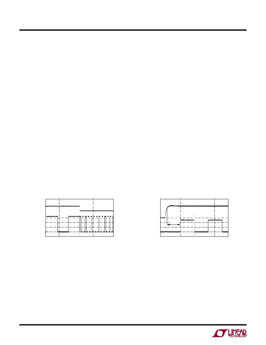
DIV
200mV/DIV
OUT
1V/DIV
10ms/DIV
6991 F05
V+ = 3.3V
RSET = 200k
V+
1V/DIV
OUT
1V/DIV
250μs/DIV
6991 F06
V+ = 2.5V
DIVCODE = 0
RSET = 50k
500μs
Figure 5. DIVCODE Change from 1 to 0
Figure 6. Typical Start-Up
OPERATION
发布紧急采购,3分钟左右您将得到回复。
相关PDF资料
LTC6992MPS6-4#TRPBF
IC OSC PWM VOLT CTLR TSOT23-6
LTC6994CDCB-2#TRPBF
IC DELAY LINE 6-DFN
LTC7541ABN#PBF
IC CMOS D/A CONV 12BIT 18-DIP
LTC7545ACG#TRPBF
IC D/ACONV MULTIPLY 12BIT 20SSOP
LTC8043EN8
IC D/A CONV 12BIT SERIAL 8-DIP
LTC8143ESW#TRPBF
IC D/A CONV 12BIT SERIAL 16-SOIC
LTM9011CY-14#PBF
IC ADC 14BIT UMODULE 140BGA
LV5609LP-E
IC CLOCK DRIVER VERTICAL 24VCT
相关代理商/技术参数
LTC6992-1
制造商:LINER 制造商全称:Linear Technology 功能描述:TimerBlox Voltage-Controlled Pulse Width Modulator (PWM)
LTC6992-2
制造商:LINER 制造商全称:Linear Technology 功能描述:TimerBlox Voltage-Controlled Pulse Width Modulator (PWM)
LTC6992-3
制造商:LINER 制造商全称:Linear Technology 功能描述:TimerBlox Voltage-Controlled Pulse Width Modulator (PWM)
LTC6992-4
制造商:LINER 制造商全称:Linear Technology 功能描述:TimerBlox Voltage-Controlled Pulse Width Modulator (PWM)
LTC6992CDCB-1#PBF
制造商:Linear Technology 功能描述:SC-Timing, Cut Tape PWM with 0% to 100% Pulse Width Control
LTC6992CDCB-1#TRMPBF
功能描述:IC OSC SILICON 1MHZ 6-DFN RoHS:是 类别:集成电路 (IC) >> 时钟/计时 - 可编程计时器和振荡器 系列:TimerBlox® 标准包装:3,000 系列:- 类型:振荡器 - 晶体 计数:- 频率:- 电源电压:2.3 V ~ 5.5 V 电流 - 电源:1.07mA 工作温度:-30°C ~ 80°C 封装/外壳:SOT-665 包装:带卷 (TR) 供应商设备封装:SS迷你型-5D 安装类型:表面贴装 其它名称:AN8955SSMTXLTR
LTC6992CDCB-1#TRPBF
功能描述:IC OSC SILICON 1MHZ 6-DFN RoHS:是 类别:集成电路 (IC) >> 时钟/计时 - 可编程计时器和振荡器 系列:TimerBlox® 产品培训模块:Lead (SnPb) Finish for COTS
Obsolescence Mitigation Program 标准包装:45 系列:- 类型:温度 - 补偿晶体振荡器(TCXO) 计数:- 频率:25MHz 电源电压:3.135 V ~ 3.465 V 电流 - 电源:1.5mA 工作温度:-40°C ~ 85°C 封装/外壳:16-SOIC(0.295",7.50mm 宽) 包装:管件 供应商设备封装:16-SOIC W 安装类型:表面贴装
LTC6992CDCB-1TRMPBF
制造商:Linear Technology 功能描述:PWM Voltage Controlled 3.81Hz-1MHz DFN6